About Our Group
The Mesoscale Materials Lab explores the structure, physical, electronic and dielectric properties of emergent solid state electronic materials, striving to advance the state-of-the-art in energy-efficient materials and devices.
The research group probes the interactions of light with matter, including inelastic light scattering revealing lattice, electronic, and magnetic phase stability. Investigators focus on the structure of ferroic/multiferroic solids and electromechanical, magnetoelectric, energy-storage, charge- and spin-storage properties. Such properties find great application in energy-efficient sensors and components for information, communications, and power systems.
Project Highlights
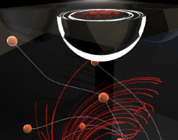
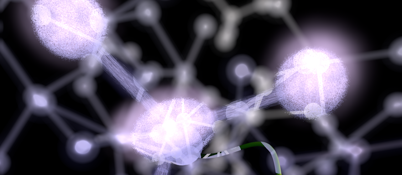
Dielectric Meta-Materials
The domain-wall structure and dynamics are found to enhance, rather than inhibit, the high-frequency performance of an intrinsically tunable material, obtaining ultra-low loss and exceptional frequency selectivity. Illustration credit: Felice Macera. Relevant publication
Mobility
Ballistic photoconduction and a mesoscopic electron free path can be attained at room temperature in a ferroelectric insulator.
Relevant Publication
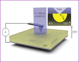
"Hot" Electrons
Nanoscale electrodes and the bulk photovoltaic effect together permit high quantum yield.
Relevant Publication
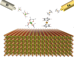
Cooler Crystallization
Solid phase epitaxy of ferroelectric perovskite oxide films can occur from amorphous films produced by atomic layer deposition at temperatures much lower than the usual bulk crystallization temperatures.
Relevant Publication
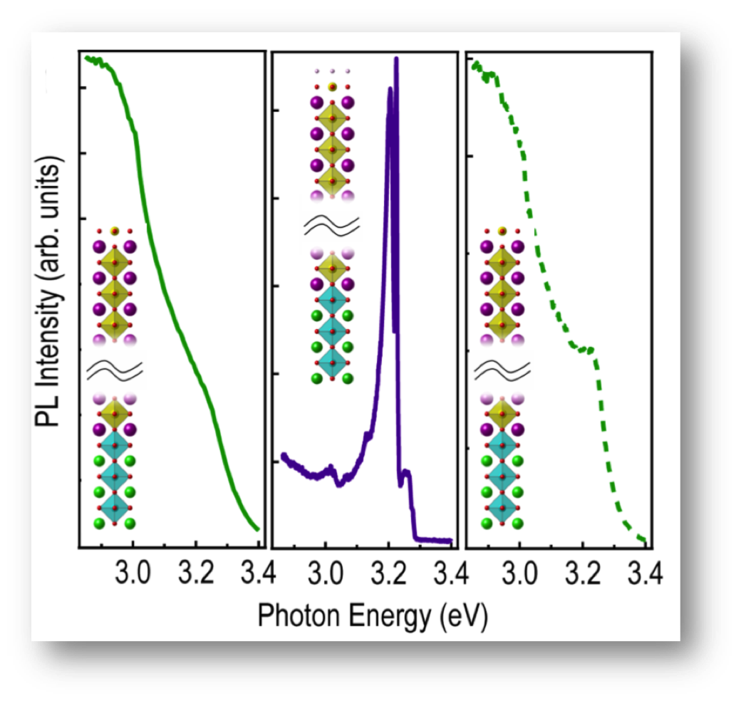
Surface Triggered Subsurface UV Light
Chemisorption and desorption of water fragments permits reversible quantum well ultraviolet luminescence. Relevant publication
Recent News
Andrew Bennett-Jackson Receives PhD
We celebrate the successful defense of Andrew Bennett-Jackson on June 15, 2022. ABJ has now joined the Applied Physics Lab at Johns Hopkins University as a postdoctoral scientist. ABJ was
Aleksandr Plokhikh Accepts Position with Lam
Alexsandr Plokhikh has accepted a position with Lam Research Corporation in Fremont, CA, after successfully defending his PhD dissertation. Founded in 1980, Lam partners with researchers and companies
Not So Inseparable After All
The drift- and diffusion-governing behaviors of photo-generated oppositely-charged carriers near surfaces of and interfaces within semiconducting and insulating solids are ubiquitous in nature, and th


